— FUJIFILM Corporation announced the launch of “ZEMATES™*1,” a new brand of photosensitive insulating materials for semiconductor back-end processes, centered on polyimide*2. The ZEMATES™ brand reflects the desire to remain a “trusted partner” that supports the future of the semiconductor industry and creates innovation together with customers by providing highly reliable materials.
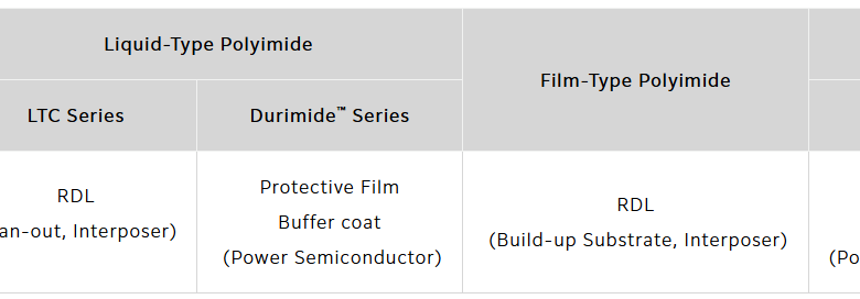
The ZEMATES™ product lineup consists of liquid-type polyimide for redistribution layers (RDL)*3 and protective films, film-type polyimide for redistribution layers and PBO (polybenzoxazole)*4 for use in protective films. These products are used as insulating layer materials in semiconductor packaging processes, covering a wide range from power semiconductors to high-performance AI semiconductors. These products, which combine excellent heat resistance and insulation properties, have earned a strong reputation for reliability. With a supply system based in Japan, the United States, and Europe, sales to semiconductor manufacturers around the world are expanding, and inquiries from new customers continue to grow.
In recent years, as the demand for improved performance and lower power consumption in semiconductors—including AI semiconductors—has increased, the need for advanced packaging that integrates multiple chips has also grown. Within this trend, the market for photosensitive insulating materials used as interlayer dielectrics in redistribution layers, which contribute to wiring miniaturization, planarization, low thermal expansion, and low dielectric constant, is expected to achieve significant growth at an annual rate of 15%*5.
Going forward, efforts will focus on further expanding sales of liquid-type polyimide as the core product, while also aiming for the early market launch of film-type polyimide developed using Fujifilm’s precision coating technology. Building on the trust earned from customers through liquid-type polyimide, the goal is to expand sales of photosensitive insulating materials to five times the level of FY2024 by FY2030.
The newly developed film-type polyimide is now compatible with PLP (panel-level packaging process), which is required for finer wiring and larger substrates in build-up substrates*6, and is expected to expand its applications from interposers*7, where liquid-type is currently used, to build-up substrates. The use of film-type polyimide enables planarization of insulating layers, suppressing surface irregularities and undulations associated with multilayer build-up substrates, thereby contributing to improved production efficiency and product quality. Notably, all polyimide products are PFAS-free*8, containing no per- or polyfluoroalkyl substances, which are of increasing environmental concern.
About Fujifilm’s Semiconductor Materials Business
Fujifilm is a global supplier of photoresists*9, photolithography-related materials*10, CMP slurries*11, post-CMP cleaners*12, thin-film chemicals*13, polyimides, high-purity process chemicals*14, and other process materials for semiconductor manufacturing from front-end to back-end processes. Fujifilm is also expanding globally with products such as WAVE CONTROL MOSAIC™*15, which includes color filter materials for image sensors.
Fujifilm will continue to contribute to the development of the semiconductor industry by providing “One-Stop Solutions” to solve customers’ issues through its broad product lineup that covers nearly all areas of the semiconductor manufacturing process, from cutting-edge to legacy nodes. The company also leverages its global stable supply system with manufacturing bases in Japan, the United States, Europe and Asia, along with its advanced research and development capabilities.
ZEMATES™ Product Lineup

- *1 ZEMATES is a registered trademark or trademark of FUJIFILM Corporation.
- *2 A material with strong heat resistance and insulation properties, used for forming semiconductors’ protective films and rewiring layer.
- *3 Wiring layer connecting small terminals of semiconductor chips to external circuits, composed of metal wiring and insulating layers. RDL stands for Redistribution Layer.
- *4 Material with high heat resistance and insulation, used for protective films and redistribution layers in semiconductors, and offering superior heat resistance and strength similar to polyimide.
- *5 Estimated by Fujifilm. Growth rate based on value from 2024 to 2030.
- *6 Multilayer substrate formed by stacking insulating and conductor layers, enabling interlayer connections using fine “laser vias” compared to conventional through-holes, achieving miniaturization and high-density wiring, especially for smartphones.
- *7 Substrate connecting multiple chips (processors, memory, etc.) in semiconductor packaging, essential for high-density mounting and connection of CPU, GPU, HBM, etc.
- *8 PFAS refers to a collective term for perfluoroalkyl compounds, polyfluoroalkyl compounds, and their salts, as defined in the OECD’s 2021 report “Reconciling Terminology of the Universe of Per- and Polyfluoroalkyl Substances: Recommendations and Practical Guidance.” Accordingly, the claim ‘PFAS-Free’ denotes the absence of substances falling within this defined group.
- *9 Material used to coat wafer substrate when circuit patterns are drawn in the process of semiconductor manufacturing.
- *10 Development solutions, cleaners and other materials used in the photolithography process of semiconductor manufacturing.
- *11 A proprietary formulation containing an abrasive that uniformly planarizes semiconductor surface, which contains a mixture of wires and insulation films of varying hardness.
- *12 Cleaners used after polishing with CMP slurry to remove particles, minute metal fragments and organic residues while protecting the metal surface.
- *13 Materials for forming low-dielectric insulation films.
- *14 High-purity chemicals used in the cleaning and drying processes. The chemicals are employed to remove contaminants during the cleaning and drying stages of semiconductor manufacturing, as well as to eliminate metals and oils during the etching process.
- *15 General term referring to a group of functional materials for controlling electromagnetic light waves in a broad range of wavelengths, including photosensitive color materials for manufacturing color filters for image sensors such as CMOS sensors, used in digital cameras and smartphones. WAVE CONTROL MOSAIC is a registered trademark or trademark of FUJIFILM Corporation.
Release Id: 89178252
If you detect any issues, problems, or errors in this press release content, kindly contact [email protected] to notify us (it is important to note that this email is the authorized channel for such matters, sending multiple emails to multiple addresses does not necessarily help expedite your request). We will respond and rectify the situation in the next 8 hours.