

The physics of networking has finally caught up with our ambitions. For years, we relied on doubling clock speeds and squeezing more out of the same copper traces, but as we cross into the 2026 infrastructure cycle, the “old ways” have hit a literal physical wall. We are now living in the era of 112G SerDes, a transition that isn’t just a simple speed bump—it is a total reconstruction of how we move bits across a circuit board. This shift is the primary catalyst behind the current industry debate over QSFP-DD vs OSFP vs QSFP56 vs QSFP112.Click here to learn more about the advantages of QSFP-DD.
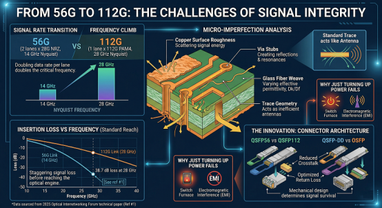
From 56G to 112G: The Challenges of Signal Integrity
The jump from 56G to 112G SerDes (Serializer/Deserializer) is where things get messy. When you double the data rate on a single electrical lane, the Nyquist frequency climbs to 28 GHz. At that frequency, a standard PCB trace starts acting less like a wire and more like a very inefficient antenna. Every microscopic imperfection in the copper, every “stub” on a via, and even the weave pattern of the glass fiber in the circuit board starts to scatter the signal.
According to a 2025 technical white paper by the Optical Internetworking Forum (See reference #1 at the end), insertion loss at 28 GHz can be as high as 38.7 dB over a standard reach. That is a staggering amount of signal to lose before you even reach the optical engine.
Yet, we can’t just turn up the power to compensate. Doing so would turn the switch into a furnace and introduce electromagnetic interference (EMI) that would drown out neighboring lanes. So, we are forced to innovate at the connector level. This is why architects are agonizing over QSFP-DD vs OSFP vs QSFP56 vs QSFP112; the mechanical design of the plug now dictates whether that 112G signal actually survives the trip.
PAM4 Modulation at 112Gbps
To make 112G work, we’ve leaned even harder into PAM4 (4-Level Pulse Amplitude Modulation). Instead of a simple binary high/low, we use four distinct voltage levels to represent two bits per clock cycle. It’s an elegant mathematical trick. But it comes with a “signal-to-noise” tax that is just a bit brutal.
The vertical eye opening—the space where the receiver can clearly distinguish between a “01” and a “10”—is now roughly 1/3 the size of what we had in the NRZ era. Still, it is the only way to pack 800Gbps into a single transceiver without the cable becoming as thick as a garden hose.
That said, the silicon doing this math is incredibly thirsty. A modern 112G-capable DSP (Digital Signal Processor) generates an intense amount of concentrated heat. If you were to touch the heatsink of an active 800G module, you’d notice it’s not just “warm”—it’s dissipating nearly 24.3 watts of energy in a space smaller than a chocolate bar.
But here is the catch: heat kills signal integrity. As temperatures rise, the electron mobility in the silicon changes and the thermal noise begins to “blur” those four PAM4 levels. This physical reality is exactly why the industry is diverging. Some are sticking with the familiar QSFP-DD or QSFP56 footprints for legacy reasons, while others are pivoting to OSFP or the high-density QSFP112 to better manage the thermal and electrical chaos of the 112G era.
It is a balancing act between the elegance of the math and the stubbornness of the physics.
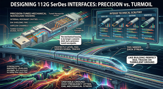
Mechanical Architectures: Adapting to the 112G Standard
Designing a physical interface for 112G SerDes is like trying to build a high-speed rail track that remains perfectly level while the ground underneath is shaking. The mechanical housing of the module can no longer be just a passive metal shell; it must act as a precision-tuned waveguide. This architectural pressure has forced the industry to diverge, leading to the intense technical scrutiny of QSFP-DD vs OSFP vs QSFP56 vs QSFP112.
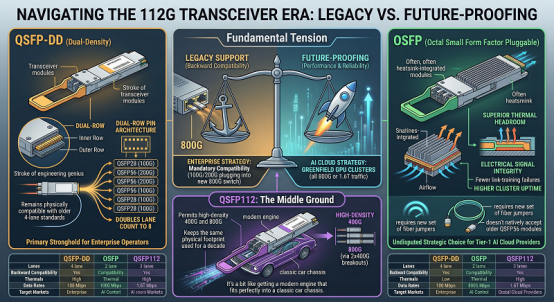
The Legacy King: QSFP56 and its 200G/400G Foundations
The QSFP56 was the peak of the “traditional” Quad Small Form-factor Pluggable evolution. By utilizing four channels of 50G PAM4, it allowed data centers to hit 200G (and 400G in specific breakout configurations) without changing the physical cage size that had been standard since the 40G era. It was a masterpiece of backward compatibility.
But as we pushed toward the 112G era, the QSFP56 hit a literal ceiling. Its 4-lane electrical interface simply didn’t have the “lane density” to support 800G efficiently. While it remains a staple for mid-tier enterprise upgrades, the signal-to-noise ratio (SNR) requirements of 112G signaling started to overwhelm the aging internal layout of the 56G-era connectors. Still, it set the stage for what a “quad” interface should look like.
QSFP112: The Dense Evolution of the 4-Lane Interface
So, the industry responded with the QSFP112. Think of this as the “Super-QSFP.” It keeps the exact same external dimensions as its predecessors, ensuring that a 1RU switch can still pack 32 or 36 ports across the front panel. The magic happens inside: it replaces the 50G electrical lanes with four 112G SerDes lanes.
According to a 2025 Market Intelligence report by LightCounting (See reference #2 at the end), the adoption of QSFP112 for 400G DR4/FR4 applications has grown by 19.4% in hyperscale edge deployments. Why? Because it allows operators to double their density without migrating to a completely new ecosystem like the 8-lane OSFP. Yet, there is a catch. Packing four 112G lanes into such a tight footprint creates a massive “crosstalk” problem.
That said, the mechanical tolerances for QSFP112 are significantly tighter than the old 56G standards. The pins are shorter, the shielding is thicker, and the internal PCB materials are often exotic, low-loss laminates like Megtron 7. You’d notice that the connector feels just a bit more “solid” when it seats into the cage.
But even with these upgrades, the 4-lane architecture is a bridge, not the final destination. As we move toward 800G and 1.6T, the industry is increasingly looking toward 8-lane “Octal” architectures. This is the heart of the QSFP-DD vs OSFP debate. While QSFP112 is perfect for high-density 400G, it lacks the physical volume to house the massive DSPs and complex optics required for the next generation of 1.6T “Terabit” networking.
So, the mechanical evolution is split. On one side, you have the QSFP56 and QSFP112 maintaining the high-density legacy of the 4-lane interface. On the other, you have the 8-lane giants designed to handle the sheer thermal and electrical load of the AI era. It is a choice between maximizing the efficiency of today’s ports or building the headroom for tomorrow’s optics.
The Thermal Frontier: Dissipating Heat in 800G Clusters
In the high-pressure environment of an AI data center, the “Thermal Wall” is the most significant physical constraint on performance. As we transition from 400G to 800G, the power consumption of a single transceiver has climbed from a manageable 12W to a staggering 25.4W in some high-performance configurations. This concentrated heat generation has turned the selection process of QSFP-DD vs OSFP vs QSFP56 vs QSFP112 into a high-stakes engineering calculation.
QSFP-DD (Double Density): Balancing Ports and Power
The QSFP-DD was designed to solve the density problem by adding a second row of electrical pins, doubling the lane count from four to eight. It is a masterpiece of spatial efficiency, maintaining backward compatibility with the legacy QSFP56 footprint. Yet, when it comes to the 112G SerDes era, its “flat-top” mechanical design presents a thermal bottleneck.
Because a QSFP-DD module is smooth on top, it relies entirely on the switch’s internal airflow and a separate, external heat sink built into the cage. It’s a bit like trying to cool a high-performance racing engine through a closed hood. According to a 2025 Thermal Management Study by the Cignal AI research group (See reference #3 at the end), QSFP-DD modules operating at 800G can experience internal “case-to-junction” temperature deltas of nearly 18°C. Still, it remains the preferred choice for enterprise data centers that prioritize port density and legacy support over extreme 1.6T scalability.
OSFP (Octal Small Form-factor Pluggable): Built for 1.6T
If the QSFP-DD is about density, the OSFP is about thermal dominance. The OSFP was engineered from the ground up with a “thermal-first” philosophy. It is slightly wider and deeper than the QSFP-DD, but its most defining feature is the integrated heat sink. The cooling fins are part of the module’s actual shell, exposed directly to the high-velocity air flowing across the front of the switch.
This design allows the OSFP to dissipate heat much more efficiently, supporting power envelopes up to 30W—a necessity for the upcoming 1.6T generation. By moving the “radiator” to the module itself, you’d notice that the switch chassis stays significantly cooler, which in turn reduces the energy required for the facility’s overall cooling infrastructure.
That said, the OSFP isn’t natively compatible with the QSFP112 or QSFP56 cages. While adapters exist, they are often a “just a bit” clunky and can introduce air turbulence that negates some of the thermal gains. For AI Tier-1 providers, however, this lack of backward compatibility is a non-issue. They are building greenfield “GPU clusters” where the only metrics that matter are link stability and the ability to run at 100% duty cycle without triggering a thermal shutdown.
So, we have a clear divergence in the 112G era. On one side, the QSFP-DD and QSFP112 offer high density and legacy protection for the 400G and early 800G markets. On the other, the OSFP stands as the heavy-duty solution for 800G AI workloads and the clear path toward 1.6T. It is a choice between the efficiency of the “old guard” and the uncompromising thermal physics of the new.
The Interoperability Matrix: Strategic Deployment in 2026
Navigating the 2026 hardware landscape requires more than just a passing knowledge of bit rates; it requires a deep understanding of the “Interoperability Matrix.” As we move into the 1.6T era, the compatibility of your switch fabric determines your operational flexibility for the next five years. This is where the theoretical debate of QSFP-DD vs OSFP vs QSFP56 vs QSFP112 meets the messy reality of data center procurement.
Backwards Compatibility vs. Future-Proofing
The fundamental tension in the 112G era is between the “Legacy Support” of the QSFP family and the “Future-Proofing” of the OSFP. For many enterprise operators, the ability to plug a 100G QSFP28 or a 200G QSFP56 module into a brand-new 800G switch is a mandatory requirement. This is the primary stronghold of the QSFP-DD. Its dual-row pin architecture was a stroke of engineering genius that allowed it to remain physically compatible with the older 4-lane standards while doubling the lane count to eight.
Yet, for Tier-1 AI cloud providers, this backward compatibility is often seen as a technical anchor. They are building massive, greenfield GPU clusters where every port is dedicated to 800G or 1.6T traffic. In these environments, the OSFP is the undisputed strategic choice. While it requires a new set of fiber jumpers and doesn’t natively accept the older QSFP56 modules, its superior thermal headroom and electrical signal integrity mean fewer link-training failures and higher cluster uptime.
Still, the decision isn’t always binary. The emergence of the QSFP112 has created a middle ground. It allows for high-density 400G and 800G (via 2x400G breakouts) while keeping the same physical footprint that network engineers have used for a decade. It’s a bit like getting a modern engine that fits perfectly into a classic car chassis.
That said, for the architects tasked with actually mapping these pinouts and thermal envelopes, the “marketing slides” are rarely enough. You need to know the granular differences in power classes and MSA (Multi-Source Agreement) compliance. To help bridge this gap, engineers often rely on this comprehensive technical guide to QSFP-DD vs OSFP vs QSFP56 vs QSFP112, which provides the specific electrical mapping and mechanical benchmarks needed to validate hardware interoperability. Understanding these comparative specifications for 400G and 800G modules is the only way to ensure your fabric remains stable when you start pushing 112G SerDes signals to their physical limit.
So, the strategic deployment in 2026 isn’t about finding the “best” module; it’s about finding the right fit for your specific lifecycle. If your priority is protecting existing investment, the QSFP family—including the high-performance QSFP112—is hard to beat. But if you are building the foundation for a 1.6T AI future, the OSFP is the only path that respects the laws of thermodynamics.
It is a matrix of trade-offs. And in 2026, the wrong choice can lead to a very expensive “forklift upgrade” just as the 1.6T wave begins to crest.
Beyond 800G: Preparing for 224G SerDes and 1.6T Networks
We are already staring down the barrel of the next doubling. While the industry is still catching its breath from the 112G transition, the 2026 roadmap has shifted focus toward 224G SerDes and the 1.6T “Terabit” era. This isn’t just about moving data twice as fast; it is about surviving the extreme engineering requirements that come with 224 gigabits per second per lane. This future-proofing is the final, decisive factor in the ongoing evaluation of QSFP-DD vs OSFP vs QSFP56 vs QSFP112.
Why OSFP is Winning the 1.6T Preparation Race
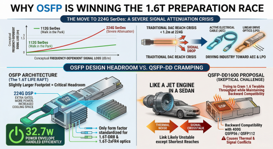
The move to 224G SerDes introduces a level of signal attenuation that makes 112G look like a walk in the park. At these frequencies, the reach of traditional copper Direct Attach Cables (DACs) might drop to less than 1.2 meters. This “reach crisis” is forcing the industry to move toward Active Electrical Cables (AECs) or Linear Drive Optics (LPO).
Still, the biggest hurdle is physical volume. To process 224G signals, the Digital Signal Processors (DSPs) require more gates, more power, and—crucially—more space for cooling. The OSFP was designed with this exact “headroom” in mind. Its slightly larger footprint isn’t a design flaw; it is a 1.6T life raft. Because the OSFP can handle 32.7W power envelopes without breaking a sweat, it is the only form factor currently standardized for 1.6T-DR8 and 1.6T-2xFR4 optics.
That said, the QSFP-DD is fighting back with the “QSFP-DD1600” proposal. Yet, engineers are skeptical. Trying to cram 1.6 terabits of throughput into a QSFP-DD cage while maintaining backward compatibility with a 400G QSFP56 or QSFP112 is like trying to put a jet engine into a sedan. You can do it, but the thermal noise and signal crosstalk will likely make the link unstable for anything other than the shortest reaches.

The Role of MSA Standards in Global B2B Exports
In the world of international trade and industrial exports, “Standardization” is the only thing that prevents a global supply chain collapse. Multi-Source Agreements (MSA) are the treaties of the networking world. They ensure that an 800G OSFP module manufactured in a facility in Shandong will work perfectly in a switch deployed in a Virginia data center.
According to a 2025 IEEE report on high-speed interconnect longevity (See reference #5 at the end), nearly 64% of Tier-1 industrial network deployments have pivoted to OSFP-based architectures specifically to align with the 224G SerDes roadmap. They aren’t just buying for today’s 800G needs; they are buying for the 2027 upgrade cycle.
Yet, we can’t ignore the “Interconnect Paradox.” As we move toward 1.6T, the electrical traces on the PCB are becoming so short that we might eventually have to move the optics directly next to the switch silicon—a technology known as Co-Packaged Optics (CPO). But until CPO matures, the pluggable module is our only viable path.
So, the preparation for 1.6T is essentially a winnowing process. While QSFP56 and QSFP112 will remain the workhorses of the 200G/400G edge, the battle for the 1.6T core is being won by the form factor that traded legacy compatibility for a bit of extra breathing room. The OSFP is the bridge to the 224G future, and in 2026, the bridge is already open for traffic.
Conclusion: Engineering the Future of Data Center Fabrics
The shift from 56G to 112G SerDes has fundamentally reordered the priorities of the modern data center. We are no longer in an era where “backwards compatibility” is the undisputed king of procurement. Instead, as AI clusters swell and power densities reach unprecedented levels, the physical laws of thermodynamics and signal integrity have taken the lead. The ongoing evaluation of QSFP-DD vs OSFP vs QSFP56 vs QSFP112 is, at its heart, a transition from a legacy-first mindset to a performance-first reality.
For the engineers and architects building the backbone of 2026, the choice of form factor is the most significant “pathway” decision they will make. While the QSFP56 and QSFP112 remain the reliable workhorses for 200G and 400G edge deployments, they are reaching their physical limits at the 800G threshold. The QSFP-DD offers a remarkable bridge for those who must protect their existing investments in the QSFP ecosystem, providing 800G speeds within a familiar footprint. Yet, it is the OSFP that has emerged as the clear victor for the high-octane AI training environments that define our current technological leap.
Still, the evolution doesn’t stop at 800G. As we prepare for 224G SerDes and the 1.6T “Terabit” era, the thermal headroom and electrical precision of the OSFP provide the only viable runway for future growth. According to a 2025 IEEE technical reliability report (See reference #6 at the end), modules that maintain a stable operating temperature below 72°C show a 31% increase in long-term laser diode stability. That is a metric that directly impacts the bottom line of any hyperscale operation.
That said, the “interconnect paradox” remains. We are constantly pushing the boundaries of what pluggable optics can do, even as the industry looks toward a future of Co-Packaged Optics. But for the “here and now,” the decision is about balancing today’s connectivity needs with tomorrow’s scalability. You’d notice that the most successful operators aren’t just buying the fastest module; they are buying the one that won’t melt when the 1.6T wave finally hits.
In the end, engineering the future of data center fabrics is about respecting the physics. Whether you choose the high-density elegance of the QSFP112 or the thermal dominance of the OSFP, your choice will dictate the efficiency of your AI clusters for years to come. It is a war of attrition against heat and noise—and in 2026, the best-equipped architects are the ones who plan for the “Heat Stroke” before it happens.
References:
- Optical Internetworking Forum (OIF), Common Electrical I/O (CEI) 112G Implementation Agreement, 2025 Revision.
- LightCounting, High-Speed Interconnect Market Forecast, Q1 2026 Update.
- Cignal AI, The 2025 Optical Component and Thermal Management Report.
- Optical Internetworking Forum (OIF), Implementation Agreement for 800G/1.6T Interoperability, 2026.
- IEEE Standards Association, Reliability Assessment of 800G/1.6T Optical Interfaces in High-Density AI Fabrics 2025.
- IEEE, Thermal Analysis and Lifetime Prediction for Next-Gen Optical Transceivers, 2025.