
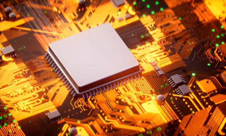
When we look at a smartphone, laptop, or AI server, everything feels solid and neatly assembled. But inside, there’s a major engineering problem most people never think about.
A silicon chip is extremely small—smaller than a fingernail—and covered with thousands of microscopic connection points. A motherboard, on the other hand, is much larger and built with connection pads that are visible and spaced far apart. These two parts live in completely different “size worlds.”
They simply can’t be connected directly.
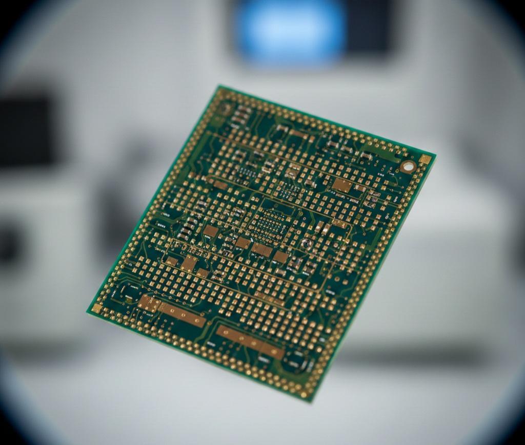
That’s where the IC substrate PCB comes in. I like to think of it as a translator. It sits between the tiny chip and the large motherboard and helps both sides communicate without stress, signal loss, or long-term damage.
In 2026, this role is more important than ever. AI processors, 5G hardware, and high-end smartphones move huge amounts of data at extreme speeds. Without advanced IC substrates, even the most powerful chip would be useless once placed into a real device.
Why Chips and Motherboards Need a Middle Layer
The first issue is connection density. Modern chips have thousands of very small contact points packed tightly together. Motherboards are not designed to handle that level of precision. The IC substrate gradually spreads those connections out so they can safely reach the board.
Heat is the second challenge. Chips heat up quickly when they work hard. Different materials expand at different rates, and if a chip were attached directly to a motherboard, that heat expansion could crack solder joints over time. The substrate acts as a cushion, absorbing stress and protecting the connection.
Then there’s signal quality. At high speeds, data behaves more like a wave than a simple on-off signal. If the path isn’t carefully designed, signals can weaken, reflect, or arrive late. IC substrates are engineered to guide these signals cleanly from the chip into the system. Without this middle layer, performance and reliability would drop fast.
What IC Substrates Are Made Of (And Why It Matters)
Not all IC substrates are built the same, and the materials used make a big difference.
BT (Bismaleimide Triazine) is a well-established material. It’s stable, affordable, and still widely used in memory chips, LEDs, and simpler electronics. It may not be cutting-edge, but it’s dependable.
ABF (Ajinomoto Build-up Film) is where high performance begins. Most modern CPUs, GPUs, and AI chips rely on ABF because it allows extremely fine wiring and many layers in a small space. From what I’ve seen, ABF is one of the main reasons today’s processors can be both powerful and compact.
Glass core substrates are the new direction the industry is moving toward. Glass expands less with heat and allows signals to travel with less distortion. This makes it very attractive for AI and data-center hardware. While still expensive and difficult to produce, glass substrates are gaining serious attention going into 2026.
How the Chip Actually Connects to the Substrate
The connection process is surprisingly delicate.
Most high-performance chips use flip-chip technology. The chip is flipped upside down and attached directly to the substrate using tiny solder bumps. This creates very short signal paths, which improves speed and reduces electrical noise.
Wire bonding is an older method where thin wires connect the chip to the substrate. It’s slower and takes more space, but it’s still useful for simpler and lower-cost devices.
On the bottom side of the substrate, a Ball Grid Array (BGA) is used. Hundreds or thousands of tiny solder balls connect the substrate to the motherboard, forming a strong and reliable link between the chip and the rest of the system.
Different Substrates for Different Jobs
Memory chips use substrates designed for consistency and speed. Even small signal errors can cause data corruption, so these designs focus on stability.
Logic chips like CPUs and AI processors use much more complex substrates. They have many layers, extremely fine traces, and strict manufacturing tolerances. These are the most challenging—and expensive—substrates to produce.
RF substrates are built for wireless communication. Used in 5G and radio systems, they are carefully tuned to handle high-frequency signals without interference or loss.
Each type is optimized for its specific role, not a one-size-fits-all solution.
How IC Substrates Are Manufactured
IC substrate manufacturing is far more advanced than regular PCB production.
Instead of traditional drilling, manufacturers use UV lasers to create microscopic holes that connect internal layers. These holes are so small that even minor defects can cause failure.
To form ultra-fine circuits, manufacturers rely on a process called modified semi-additive processing (mSAP). Rather than removing large amounts of copper, they build up precise copper traces layer by layer.
Because of this precision, IC substrate factories operate under cleanroom conditions. Dust particles that wouldn’t matter in normal PCB manufacturing can ruin a substrate. That’s why these facilities look more like semiconductor fabs than typical board factories.
Why This “Bridge” Matters More Than Ever
IC substrate PCBs don’t get much attention, but they quietly decide how thin, fast, and reliable modern electronics can be.
As devices continue to shrink and chips grow more powerful, substrates are doing more work in less space. The AI boom, in particular, depends heavily on better substrate technology to move data faster and manage heat more effectively.
From my perspective, the future of computing isn’t just about better chips. It’s also about better bridges—smartly designed IC substrates that connect those chips to the real world without holding them back.