The Atlas® G6 system delivers smaller spot size, higher signal sensitivity and enhanced precision for next generation gate-all-around and high bandwidth memory device production
WILMINGTON, Mass.–(BUSINESS WIRE)–$ONTO—Onto Innovation Inc. (NYSE: ONTO) today introduced the Atlas® G6 optical critical dimension (OCD) metrology system, designed to address the growing complexity of process control in advanced semiconductor nodes. As the industry transitions to second generation gate-all-around (GAA) logic and future vertical gate DRAM architectures to support AI applications, manufacturers face tighter structural dimensions, shrinking by up to 30% per generation. These smaller geometries demand greater precision in controlling individual nanowire measurements in GAA and smaller DRAM cell block sizes for high bandwidth memory (HBM). The Atlas G6 system introduces advanced optical technologies that deliver measurement accuracy and the small spot size needed to support these evolving requirements, enabling robust process control for next generation devices. The Atlas G6 system has already secured multiple production orders from leading logic and memory manufacturers.
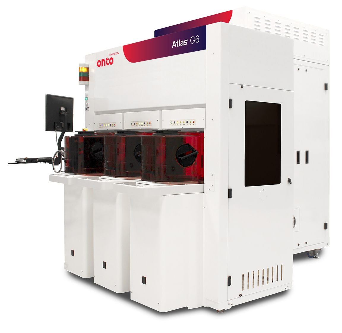

The Atlas G6 system delivers enhanced signal to noise performance even with significantly smaller spot sizes, enabling new and critical metrology capabilities for GAA and HBM technologies. For GAA devices, precise control of each individual nanowire is critical to ensure electrical performance required to meet higher transistor speeds and lower power consumption targets of next generation devices. The Atlas G6 system addresses this challenge with enhanced real-time stabilization technologies that improve measurement precision and accuracy.
For HBM, smaller DRAM cell block sizes boost bandwidth efficiency, reduce power consumption, and improve latency. The Atlas G6 system’s smaller spot size allows for direct on-device measurements in DRAM cell blocks, enabling tighter process windows and ultimately helping to improve yield and long-term reliability. Also, the system introduces an additional data channel, which when combined with Onto’s proprietary Ai Diffract™ OCD analysis software and model-guided machine learning algorithms, strengthens recipe robustness and shortens time to solution.
“As the latest evolution of our industry-leading and award-winning Atlas family, the Atlas G6 system provides control of device features that were previously difficult to measure,” said Ido Dolev, executive vice president of product solutions for Onto Innovation. “Advancements in AI technologies depend on innovations in process control, and the Atlas G6 metrology system sets a new benchmark for optical metrology performance.”
To learn more about the Atlas G6 metrology system, visit our booth L0628 at SEMICON® Taiwan, contact us or reach out to your local sales team.
About Onto Innovation Inc.
Onto Innovation is a leader in process control, combining global scale with an expanded portfolio of leading-edge technologies that includes un-patterned wafer quality, 3D metrology spanning chip features from nanometer scale transistors to large die interconnects, macro defect inspection of wafers and packages, metal interconnect composition, factory analytics, and lithography for advanced semiconductor packaging.
Our breadth of offerings across the entire semiconductor value chain combined with our connected thinking approach results in a unique perspective to help solve our customers’ most difficult yield, device performance, quality, and reliability issues. Onto Innovation strives to optimize customers’ critical path of progress by making them smarter, faster and more efficient. Headquartered in Wilmington, Massachusetts, Onto Innovation supports customers with a worldwide sales and service organization.
Additional information can be found at www.ontoinnovation.com.
Forward-Looking Statements
This press release contains forward-looking statements within the meaning of the Private Securities Litigation Reform Act of 1995 (the “Act”) which include statements relating to Onto Innovation’s business momentum and future growth; technology development, product introduction and acceptance of Onto Innovation’s products and services; capabilities of Onto Innovation’s products and customer service and their benefits to customers; Onto Innovation’s manufacturing practices and ability to both deliver products and services consistent with our customers’ demands and expectations and strengthen its market position, Onto Innovation’s expectations regarding the semiconductor market outlook as well as other matters that are not purely historical data. Onto Innovation wishes to take advantage of the “safe harbor” provided for by the Act and cautions that actual results may differ materially from those projected as a result of various factors, including risks and uncertainties, many of which are beyond Onto Innovation’s control. Such factors include, but are not limited to, the Company’s ability to leverage its resources to improve its position in its core markets; its ability to weather difficult economic environments; its ability to open new market opportunities and target high-margin markets; the strength/weakness of the back-end and/or front-end semiconductor market segments; fluctuations in customer capital spending; the Company’s ability to effectively manage its supply chain and adequately source components from suppliers to meet customer demand; the effects of political, economic, legal, and regulatory changes, including tariffs and trade disputes, or conflicts on the Company’s global operations; its ability to adequately protect its intellectual property rights and maintain data security; the effects of natural disasters or public health emergencies on the global economy and on the Company’s customers, suppliers, employees, and business; its ability to effectively maneuver global trade issues and changes in trade and export regulations, tariffs and license policies; the Company’s ability to maintain relationships with its customers and manage appropriate levels of inventory to meet customer demands; and the Company’s ability to successfully integrate acquired businesses and technologies. Additional information and considerations regarding the risks faced by Onto Innovation are available in Onto Innovation’s Form 10-K report for the year ended December 28, 2024, and other filings with the Securities and Exchange Commission. As the forward-looking statements are based on Onto Innovation’s current expectations, the Company cannot guarantee any related future results, levels of activity, performance, or achievements. Onto Innovation does not assume any obligation to update the forward-looking information contained in this press release, except as required by law.
Source: Onto Innovation Inc.
ONTO-IP
Contacts
Investor Relations:
Sidney Ho, +1 408.376.9163
[email protected]